Introduction
General Product Information
The RT8297B is a high efficiency, monolithic synchronous step-down DC/DC converter that operates at 800kHz and delivers up to 1.5A output current from a 4V to 17V input supply. The RT8297B’s current mode architecture allows the transient response to be optimized. Cycle-by-cycle current limit provides protection against shorted outputs and soft-start eliminates input current surge during start-up. Fault conditions also include output under voltage protection, output over voltage protection, and thermal shutdown. The low current (<5μA) shutdown mode provides output disconnect, enabling easy power management in battery-powered systems. The RT8297B is available in a WDFN-8L 2x2 package.
Product Feature
- 4V to 17V Input Voltage Range
- 1.5A Output Current
- Internal N-MOSFETs
- Current Mode Control
- Fixed Frequency Operation : 800kHz
- Output Adjustable from 0.8V to 12V
- Up to 95% Efficiency
- Internal Compensation
- Stable with Low ESR Ceramic Output Capacitors
- Cycle-by-Cycle Over Current Protection
- Input Under Voltage Lockout
- Output Under Voltage Protection
- Output Over Voltage Protection
- Power Good Indicator
- Thermal Shutdown Protection
Key Performance Summary Table
|
Key features
|
Evaluation board number: PCB005_V1
|
|
Default Input Voltage
|
12V
|
|
Max Output Current
|
1.5A
|
|
Default Output Voltage
|
3.3V
|
|
Default Marking & Package Type
|
RT8297BZQW (WDFN-8L 2x2)
|
|
Operation Frequency
|
Steady 800kHz at all load currents
|
|
Other Key Features
|
4V to 17V Input Voltage Range
Power Good Indicator
Tiny WDFN-8L 2x2 package
|
|
Protection
|
Over Current Protection
Hiccup Mode Output Under-Voltage & Over-Voltage Protection
Thermal Shutdown
|
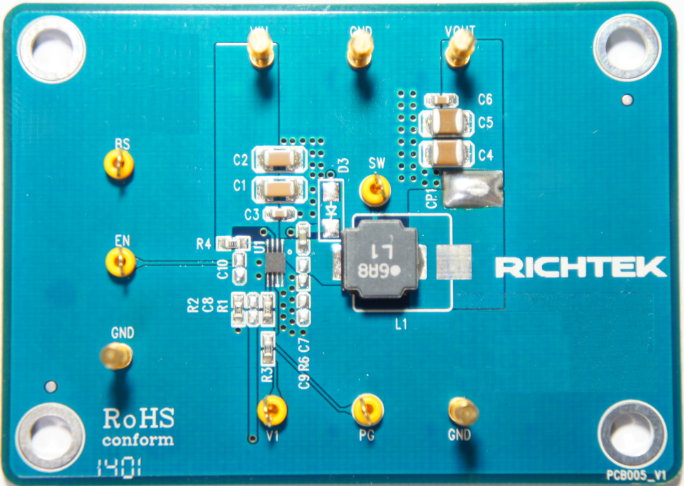
Bench Test Setup Conditions
Headers Description and Placement
Please carefully inspect the EVB IC and external components, comparing them to the following Bill of Materials, to ensure that all components are installed and undamaged. If any components are missing or damaged during transportation, please contact the distributor or send e-mail to evb_service@richtek.com.
Test Points
The EVB is provided with the test points and pin names listed in the table below.
|
Test point/
Pin name
|
Signal
|
Comment (expected waveforms or voltage levels on test points)
|
|
VIN
|
Input voltage
|
Input voltage range= 4V to 17V
|
|
VOUT
|
Output voltage
|
Default output voltage = 3.3V
Output voltage range= 0.8V to 12V
(see ‘’ Output Voltage Setting’’ section for changing output voltage level)
|
|
SW
|
Switching node test point
|
SW waveform
|
|
EN
|
Enable test point
|
Enable signal. EN is automatically pulled high (by R4) to enable operation. Connect EN low to disable operation.
|
|
BS
|
Boot strap supply test point
|
Floating supply voltage for the high-side N-MOSFET switch
|
|
PG
|
Power Good test point
|
Power Good Indicator
|
|
V1
|
External Voltage for PG
|
External voltage terminal for PG pull-up voltage.
|
|
GND
|
Ground
|
Ground
|
Power-up & Measurement Procedure
1.Apply a 12V nominal input power supply (4V < VIN < 17V) to the VIN and GND terminals.
2.The EN voltage is pulled to logic high by R4 (100kΩ to VIN) to enable operation. Drive EN high (>2.5V) to enable operation or low (<0.4V) to disable operation.
3.Verify the output voltage (approximately 3.3V) between VOUT and GND.
4.Connect an external load up to 1.5A to the VOUT and GND terminals and verify the output voltage and current.
Output Voltage Setting
Set the output voltage with the resistive divider (R1, R2) between VOUT and GND with the midpoint connected to FB. The output is set by the following formula:
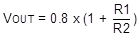
The installed VOUT capacitors (C4, C5) are 22μF, 16V X5R ceramic types. Do not exceed their operating voltage range and consider their voltage coefficient (capacitance vs. bias voltage) and ensure that the capacitance is sufficient to maintain stability and provide sufficient transient response for your application. This can be verified by checking the output transient response as described in the RT8297 IC datasheet.
Schematic, Bill of Materials and Board Layout
EVB Schematic Diagram
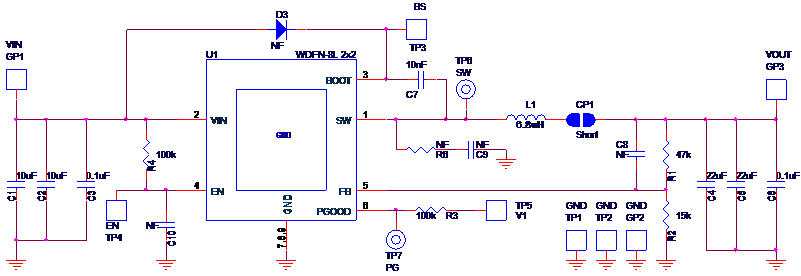
C1, C2: 10μF/50V/X5R, 1206, TDK C3216X5R1H106K
C4, C5: 22μF/16V/X5R, 1210, Murata GRM32ER61C226K
L1: 6.8μH TAIYO YUDEN NR8040T6R8N, DCR=25mΩ
Bill of Materials
|
Reference
|
Qty
|
Part number
|
Description
|
Package
|
Manufacture
|
|
U1
|
1
|
RT8297BZQW
|
DC-DC Converter
|
WDFN-8L 2x2
|
Richtek
|
|
C1, C2
|
2
|
C3216X5R1H106K160AB
|
10μF/±10%/50V/X5R
Ceramic Capacitor
|
1206
|
TDK
|
|
C4, C5
|
2
|
GRM32ER61C226KE20#
|
22μF/±10%/16V/X5R
Ceramic Capacitor
|
1210
|
Murata
|
|
C7
|
1
|
GRM32MR71H103KA01#
|
10nF/±10%/50V/X7R
Ceramic Capacitor
|
0603
|
Murata
|
|
C3, C6
|
2
|
C1608X7R1H104K080AA
|
0.1μF/±10%/50V/X7R
Ceramic Capacitor
|
0603
|
TDK
|
|
C8, C9, C10
|
0
|
|
Not Installed
|
0603
|
|
|
L1
|
1
|
NR8040T6R8N
|
6.8uH/3.7A/±30%,
DCR=25mΩ, Inductor
|
8mmx8mmx4mm
|
TAIYO YUDEN
|
|
R1
|
1
|
|
47kΩ/±1%, Resistor
|
0603
|
|
|
R2
|
1
|
|
15kΩ/±1%, Resistor
|
0603
|
|
|
R3, R4
|
1
|
|
100kΩ/±1%, Resistor
|
0603
|
|
|
CP1
|
1
|
|
Short
|
|
|
|
D3, R6
|
0
|
|
Not Installed
|
|
|
|
TP
|
6
|
|
Test Pin
|
|
|
|
GP
|
4
|
|
Golden Pin
|
|
|
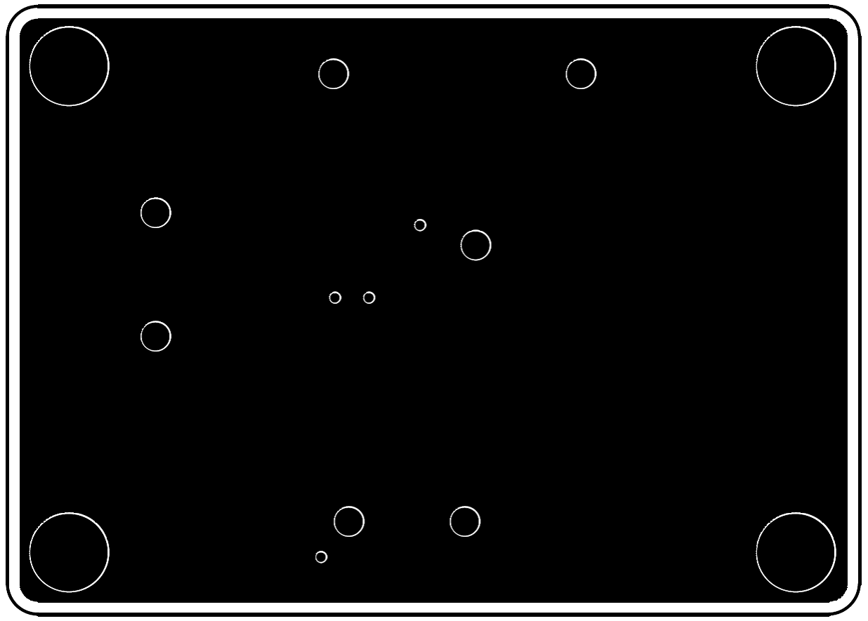
EVB Layout
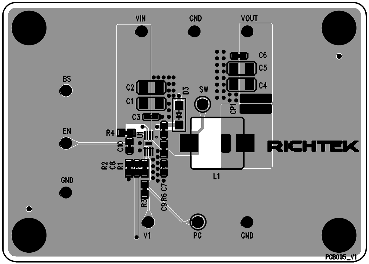
Top View (1stlayer)
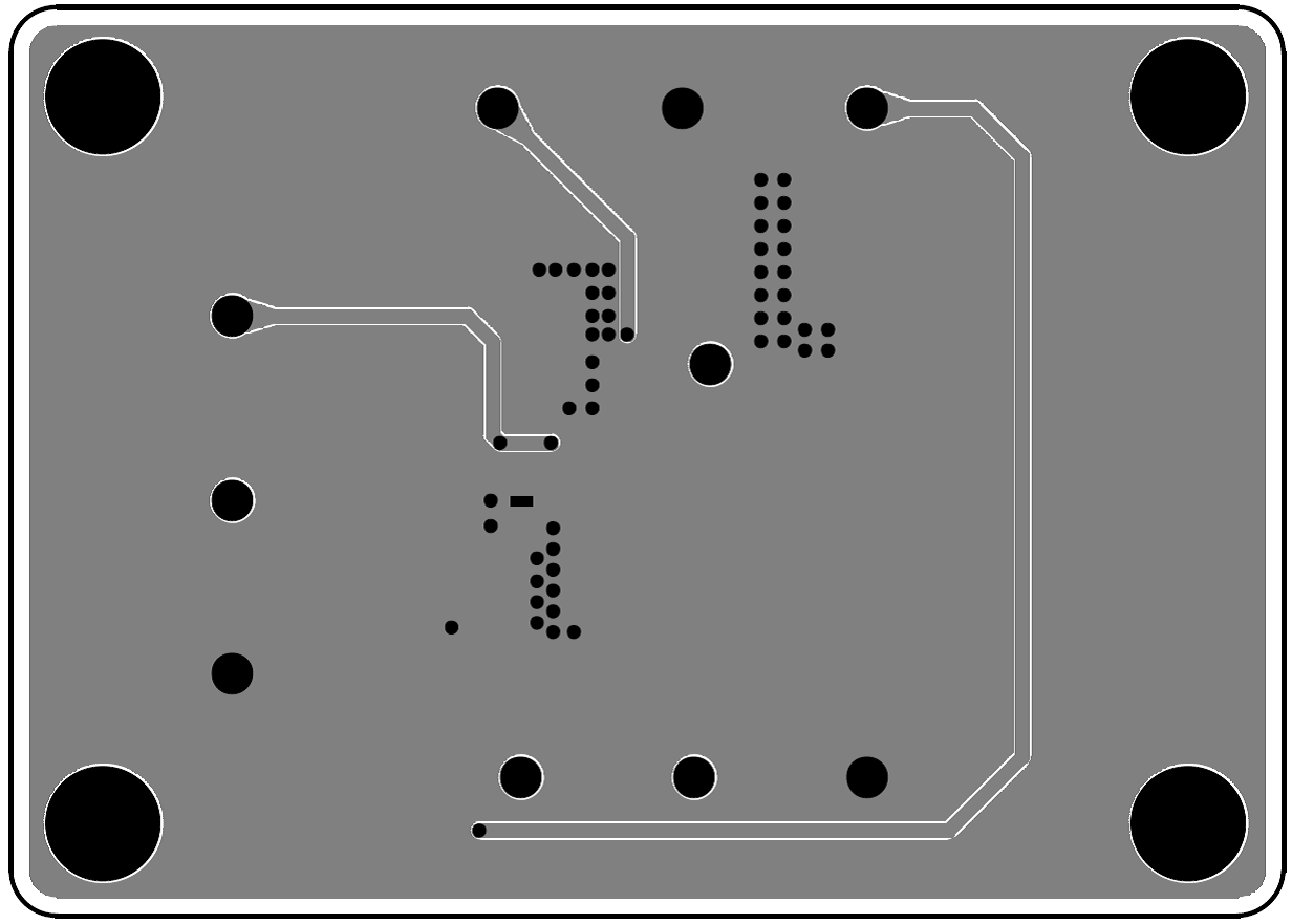
Bottom View (4th Layer)
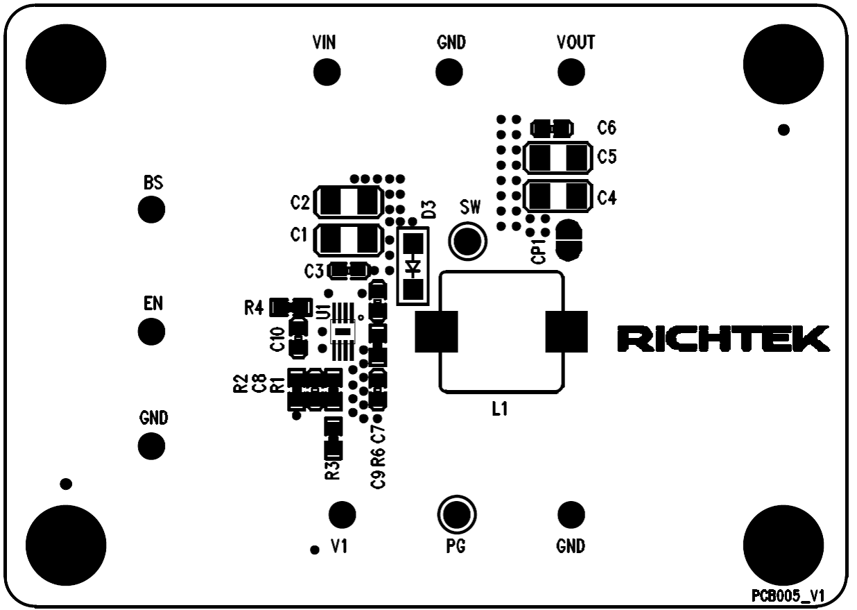
Component Placement Guide—Component Side (1stlayer)
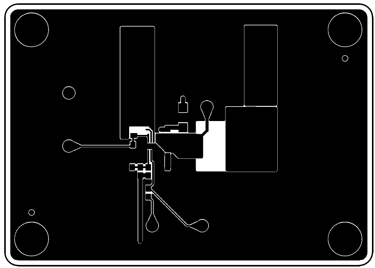
PCB Layout—Component Side (1stLayer)
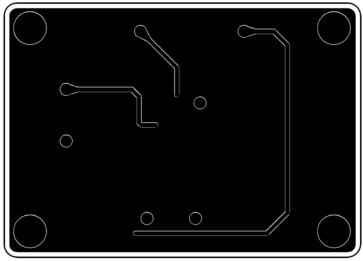
PCB Layout—Inner Side (2ndlayer)
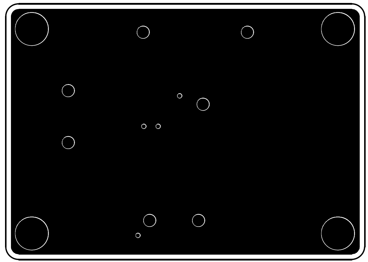
PCB Layout—Inner Side (3rd layer)
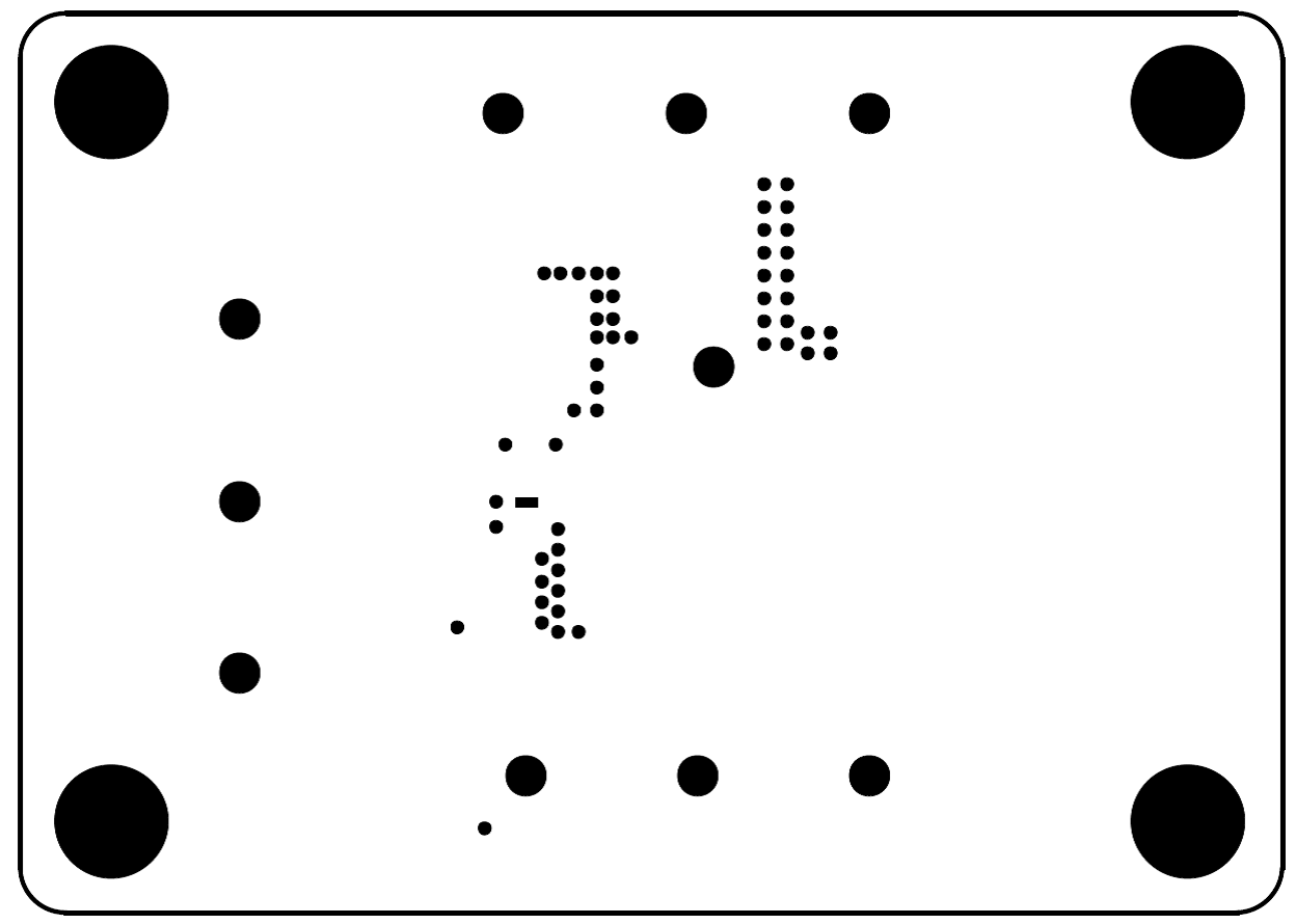
Component Placement Guide—Bottom Side (4th Layer)
PCB Layout—Bottom Side (4th Layer)